In a fascinating turn of events, a Reddit user stumbled upon a silicon wafer in a trash can near TSMC’s Fab 16 in Nanjing, China. While the practice of chip binning—where chips are categorized based on their performance post-manufacturing—typically involves high-end chips being sold at premium prices, this scene was quite different. The wafer, designed for testing purposes and not suitable for producing market-ready chips, sparks curiosity about the manufacturing processes of semiconductor giants.
After chips are manufactured, they undergo rigorous testing to evaluate critical parameters such as clock speed and power consumption. Based on their performance, chips are sorted into different categories, or "bins," with top-performing models commanding higher prices. Chips failing to meet full specifications can still find new life in lower tiers, such as labeling a processor with one defective core as a seven-core chip.
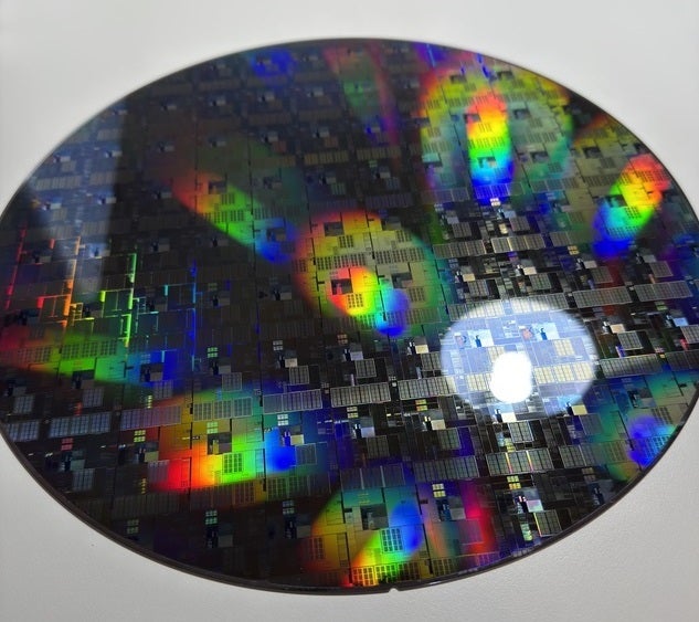
Test silicon wafer discovered by Reddit user AVX512-VNNI in a dumpster near TSMC's Fab 16. | Image credit-Reddit subscriber AVX512-VNNI
The wafer discovered cannot be used to manufacture AI chips, like those utilized by OpenAI, due to its nature as a test wafer featuring dummy circuitry. These wafers are critical for validating the lithographic equipment used to create the intricate patterns on functioning silicon wafers that are eventually sliced into semiconductor chips.
Among the Reddit comments, there were playful suggestions on how to repurpose the wafer. Some users proposed framing it as a piece of art, while others joked about using diamond-tipped kitchen tools to attempt to slice it. Given the wafer’s significance in driving technology innovation, it could indeed make a compelling conversation starter in any tech enthusiast’s collection.
The light-hearted exchange highlights both the serious nature of semiconductor manufacturing and the curiosity and creativity that such a unique find can inspire.